本文转载自:孤独的单刀的CSDN博客
打包2个AXI4-Full接口的IP(一主一从),来对其提供的仿真和原始代码学习一番。限于篇幅,将分2篇文章写完,本文写AXI4-Full接口。AXI4-Full接口的源码基本与AXI4-Lite接口的源码一致,不过多了突发传输控制的相关信号,建议配合AXI4-Lite接口源码分析文章一并查看,有助于理解。
1、调用IP
首先新建一个工程,然后点击Tools-----create and package new ip

点击Next

选择选项4,点击Next,各选项含义:
1---将当前工程打包为IP核
2----将当前工程的模块设计打包为IP核
3----将一个特定的文件夹目录打包为IP核
4----创建一个带AXI接口的IP核

填写IP信息(基本不修改,只改下名称方便后续管理),点击Next

选择Full接口,接口类型选择从机slave,数据位宽32位,存储器大小选择64即可,然后点击Next

这里选择第3个,使用AXI4 VIP来验证IP,然后点击Next。(AXI4 VIP是XILINX的一个IP核,该IP核可以提供多种连接方式来对AXI接口进行验证,用起来很是贴心方便,我们后面会写相关文章,还请期待。)

到此就生成了一个slave接口的验证工程。不着急仿真,先跟它耍耍。整个工程的结构如下:

双击上个表示的BD模块,打开工程框图,如下:

整个工程由两部分构成:1、我们打包的IP,该IP的接口是AIX4-Full-slave;2、AXI Verification IP,这是一个AXI的验证IP,提供多种验证方式,功能很强大,双击这个IP,看看它的内置定制信息:
可以看到,它可选选择接口模式来实现主机或从机或直通功能;可选协议类型,地址位宽,数据位宽等。我们这里不动它,直接cancel。

2、Slave接口的源码分析
在如下路径下有生成的接口源码:

接下来双击打开,我们一探究竟。(由于源码较长700行,一次性展开不利于阅读,我接下来分块进行讲解)
NO.1----模块参数、输入输出信号:
参数主要是数据、地址、ID的位宽;
接口即为标准的AXI4-Full的标准接口,忘记了信号定义的可以看这里:带你快速入门AXI4总线--AXI4-Full篇(1)----AXI4-Full总线
`timescale 1 ns / 1 ps

	module myip_axi4_Full_slave_v1_0_S00_AXI #
	(
		// Users to add parameters here

		// User parameters ends
		// Do not modify the parameters beyond this line

		// Width of ID for for write address, write data, read address and read data
		parameter integer C_S_AXI_ID_WIDTH	= 1,
		// Width of S_AXI data bus
		parameter integer C_S_AXI_DATA_WIDTH	= 32,
		// Width of S_AXI address bus
		parameter integer C_S_AXI_ADDR_WIDTH	= 6,
		// Width of optional user defined signal in write address channel
		parameter integer C_S_AXI_AWUSER_WIDTH	= 0,
		// Width of optional user defined signal in read address channel
		parameter integer C_S_AXI_ARUSER_WIDTH	= 0,
		// Width of optional user defined signal in write data channel
		parameter integer C_S_AXI_WUSER_WIDTH	= 0,
		// Width of optional user defined signal in read data channel
		parameter integer C_S_AXI_RUSER_WIDTH	= 0,
		// Width of optional user defined signal in write response channel
		parameter integer C_S_AXI_BUSER_WIDTH	= 0
	)
	(
		// Users to add ports here

		// User ports ends
		// Do not modify the ports beyond this line

		// Global Clock Signal
		input wire  S_AXI_ACLK,
		// Global Reset Signal. This Signal is Active LOW
		input wire  S_AXI_ARESETN,
		// Write Address ID
		input wire [C_S_AXI_ID_WIDTH-1 : 0] S_AXI_AWID,
		// Write address
		input wire [C_S_AXI_ADDR_WIDTH-1 : 0] S_AXI_AWADDR,
		// Burst length. The burst length gives the exact number of transfers in a burst
		input wire [7 : 0] S_AXI_AWLEN,
		// Burst size. This signal indicates the size of each transfer in the burst
		input wire [2 : 0] S_AXI_AWSIZE,
		// Burst type. The burst type and the size information,
    // determine how the address for each transfer within the burst is calculated.
		input wire [1 : 0] S_AXI_AWBURST,
		// Lock type. Provides additional information about the
    // atomic characteristics of the transfer.
		input wire  S_AXI_AWLOCK,
		// Memory type. This signal indicates how transactions
    // are required to progress through a system.
		input wire [3 : 0] S_AXI_AWCACHE,
		// Protection type. This signal indicates the privilege
    // and security level of the transaction, and whether
    // the transaction is a data access or an instruction access.
		input wire [2 : 0] S_AXI_AWPROT,
		// Quality of Service, QoS identifier sent for each
    // write transaction.
		input wire [3 : 0] S_AXI_AWQOS,
		// Region identifier. Permits a single physical interface
    // on a slave to be used for multiple logical interfaces.
		input wire [3 : 0] S_AXI_AWREGION,
		// Optional User-defined signal in the write address channel.
		input wire [C_S_AXI_AWUSER_WIDTH-1 : 0] S_AXI_AWUSER,
		// Write address valid. This signal indicates that
    // the channel is signaling valid write address and
    // control information.
		input wire  S_AXI_AWVALID,
		// Write address ready. This signal indicates that
    // the slave is ready to accept an address and associated
    // control signals.
		output wire  S_AXI_AWREADY,
		// Write Data
		input wire [C_S_AXI_DATA_WIDTH-1 : 0] S_AXI_WDATA,
		// Write strobes. This signal indicates which byte
    // lanes hold valid data. There is one write strobe
    // bit for each eight bits of the write data bus.
		input wire [(C_S_AXI_DATA_WIDTH/8)-1 : 0] S_AXI_WSTRB,
		// Write last. This signal indicates the last transfer
    // in a write burst.
		input wire  S_AXI_WLAST,
		// Optional User-defined signal in the write data channel.
		input wire [C_S_AXI_WUSER_WIDTH-1 : 0] S_AXI_WUSER,
		// Write valid. This signal indicates that valid write
    // data and strobes are available.
		input wire  S_AXI_WVALID,
		// Write ready. This signal indicates that the slave
    // can accept the write data.
		output wire  S_AXI_WREADY,
		// Response ID tag. This signal is the ID tag of the
    // write response.
		output wire [C_S_AXI_ID_WIDTH-1 : 0] S_AXI_BID,
		// Write response. This signal indicates the status
    // of the write transaction.
		output wire [1 : 0] S_AXI_BRESP,
		// Optional User-defined signal in the write response channel.
		output wire [C_S_AXI_BUSER_WIDTH-1 : 0] S_AXI_BUSER,
		// Write response valid. This signal indicates that the
    // channel is signaling a valid write response.
		output wire  S_AXI_BVALID,
		// Response ready. This signal indicates that the master
    // can accept a write response.
		input wire  S_AXI_BREADY,
		// Read address ID. This signal is the identification
    // tag for the read address group of signals.
		input wire [C_S_AXI_ID_WIDTH-1 : 0] S_AXI_ARID,
		// Read address. This signal indicates the initial
    // address of a read burst transaction.
		input wire [C_S_AXI_ADDR_WIDTH-1 : 0] S_AXI_ARADDR,
		// Burst length. The burst length gives the exact number of transfers in a burst
		input wire [7 : 0] S_AXI_ARLEN,
		// Burst size. This signal indicates the size of each transfer in the burst
		input wire [2 : 0] S_AXI_ARSIZE,
		// Burst type. The burst type and the size information,
    // determine how the address for each transfer within the burst is calculated.
		input wire [1 : 0] S_AXI_ARBURST,
		// Lock type. Provides additional information about the
    // atomic characteristics of the transfer.
		input wire  S_AXI_ARLOCK,
		// Memory type. This signal indicates how transactions
    // are required to progress through a system.
		input wire [3 : 0] S_AXI_ARCACHE,
		// Protection type. This signal indicates the privilege
    // and security level of the transaction, and whether
    // the transaction is a data access or an instruction access.
		input wire [2 : 0] S_AXI_ARPROT,
		// Quality of Service, QoS identifier sent for each
    // read transaction.
		input wire [3 : 0] S_AXI_ARQOS,
		// Region identifier. Permits a single physical interface
    // on a slave to be used for multiple logical interfaces.
		input wire [3 : 0] S_AXI_ARREGION,
		// Optional User-defined signal in the read address channel.
		input wire [C_S_AXI_ARUSER_WIDTH-1 : 0] S_AXI_ARUSER,
		// Write address valid. This signal indicates that
    // the channel is signaling valid read address and
    // control information.
		input wire  S_AXI_ARVALID,
		// Read address ready. This signal indicates that
    // the slave is ready to accept an address and associated
    // control signals.
		output wire  S_AXI_ARREADY,
		// Read ID tag. This signal is the identification tag
    // for the read data group of signals generated by the slave.
		output wire [C_S_AXI_ID_WIDTH-1 : 0] S_AXI_RID,
		// Read Data
		output wire [C_S_AXI_DATA_WIDTH-1 : 0] S_AXI_RDATA,
		// Read response. This signal indicates the status of
    // the read transfer.
		output wire [1 : 0] S_AXI_RRESP,
		// Read last. This signal indicates the last transfer
    // in a read burst.
		output wire  S_AXI_RLAST,
		// Optional User-defined signal in the read address channel.
		output wire [C_S_AXI_RUSER_WIDTH-1 : 0] S_AXI_RUSER,
		// Read valid. This signal indicates that the channel
    // is signaling the required read data.
		output wire  S_AXI_RVALID,
		// Read ready. This signal indicates that the master can
    // accept the read data and response information.
		input wire  S_AXI_RREADY
	);
NO.2----寄存器定义:
主要是对AXI4的输出端口的寄存器定义,避免直接对输出端口操作;
wrap突发模式的相关信号,包括地址、长度、使能等(在本次验证中没有使用到wrap突发模式,所以我直接无视它了);
memory相关信号,这个memory等于是构造了一个双口RAM,将主机发送过来的数据寄存起来。
// AXI4FULL signals
	reg [C_S_AXI_ADDR_WIDTH-1 : 0] 	axi_awaddr;
	reg  							axi_awready;
	reg  							axi_wready;
	reg [1 : 0] 					axi_bresp;
	reg [C_S_AXI_BUSER_WIDTH-1 : 0]	axi_buser;
	reg  							axi_bvalid;
	reg [C_S_AXI_ADDR_WIDTH-1 : 0] 	axi_araddr;
	reg  							axi_arready;
	reg [C_S_AXI_DATA_WIDTH-1 : 0] 	axi_rdata;
	reg [1 : 0] 					axi_rresp;
	reg  							axi_rlast;
	reg [C_S_AXI_RUSER_WIDTH-1 : 0]	axi_ruser;
	reg  							axi_rvalid;

//wrap突发模式信号
	// aw_wrap_en determines wrap boundary and enables wrapping
	wire aw_wrap_en;
	// ar_wrap_en determines wrap boundary and enables wrapping
	wire ar_wrap_en;
	// aw_wrap_size is the size of the write transfer, the
	// write address wraps to a lower address if upper address
	// limit is reached
	wire [31:0]  aw_wrap_size ;
	// ar_wrap_size is the size of the read transfer, the
	// read address wraps to a lower address if upper address
	// limit is reached
	wire [31:0]  ar_wrap_size ;
	// The axi_awv_awr_flag flag marks the presence of write address valid

	reg axi_awv_awr_flag;
	//The axi_arv_arr_flag flag marks the presence of read address valid
	reg axi_arv_arr_flag;
	// The axi_awlen_cntr internal write address counter to keep track of beats in a burst transaction
	reg [7:0] axi_awlen_cntr;
	//The axi_arlen_cntr internal read address counter to keep track of beats in a burst transaction
	reg [7:0] axi_arlen_cntr;
	reg [1:0] axi_arburst;
	reg [1:0] axi_awburst;
	reg [7:0] axi_arlen;
	reg [7:0] axi_awlen;
	//local parameter for addressing 32 bit / 64 bit C_S_AXI_DATA_WIDTH
	//ADDR_LSB is used for addressing 32/64 bit registers/memories
	//ADDR_LSB = 2 for 32 bits (n downto 2)
	//ADDR_LSB = 3 for 42 bits (n downto 3)

	localparam integer ADDR_LSB = (C_S_AXI_DATA_WIDTH/32)+ 1;
	localparam integer OPT_MEM_ADDR_BITS = 3;
	localparam integer USER_NUM_MEM = 1;
	//----------------------------------------------
	//-- Signals for user logic memory space example
	//------------------------------------------------
	wire [OPT_MEM_ADDR_BITS:0]		 	mem_address;
	wire [USER_NUM_MEM-1:0] 			mem_select;
	reg [C_S_AXI_DATA_WIDTH-1:0] 		mem_data_out[0 : USER_NUM_MEM-1];

	genvar i;
	genvar j;
	genvar mem_byte_index;
NO.3----wire信号赋值:
对AXI4的输出信号赋值,避免直接对其进行操作。
	// I/O Connections assignments
	assign S_AXI_AWREADY = axi_awready;
	assign S_AXI_WREADY	= axi_wready;
	assign S_AXI_BRESP	= axi_bresp;
	assign S_AXI_BUSER	= axi_buser;
	assign S_AXI_BVALID	= axi_bvalid;
	assign S_AXI_ARREADY = axi_arready;
	assign S_AXI_RDATA	= axi_rdata;
	assign S_AXI_RRESP	= axi_rresp;
	assign S_AXI_RLAST	= axi_rlast;
	assign S_AXI_RUSER	= axi_ruser;
	assign S_AXI_RVALID	= axi_rvalid;
	assign S_AXI_BID = S_AXI_AWID;
	assign S_AXI_RID = S_AXI_ARID;
//wrap突发模式信号
	assign  aw_wrap_size = (C_S_AXI_DATA_WIDTH/8 * (axi_awlen));
	assign  ar_wrap_size = (C_S_AXI_DATA_WIDTH/8 * (axi_arlen));
	assign  aw_wrap_en = ((axi_awaddr & aw_wrap_size) == aw_wrap_size)? 1'b1: 1'b0;
	assign  ar_wrap_en = ((axi_araddr & ar_wrap_size) == ar_wrap_size)? 1'b1: 1'b0;
NO.4----写地址通道:
完成写地址通道的握手,即根据主机给出的握手信号来拉高axi_awready,并拉高axi_awv_awr_flag信号,表示从机进入了被写入数据的过程。
	// Implement axi_awready generation

	// axi_awready is asserted for one S_AXI_ACLK clock cycle when both
	// S_AXI_AWVALID and S_AXI_WVALID are asserted. axi_awready is
	// de-asserted when reset is low.

	always @( posedge S_AXI_ACLK )
	begin
	  if ( S_AXI_ARESETN == 1'b0 )
	    begin
	      axi_awready <= 1'b0;
	      axi_awv_awr_flag <= 1'b0;
	    end
	  else
	    begin
	      if (~axi_awready && S_AXI_AWVALID && ~axi_awv_awr_flag && ~axi_arv_arr_flag)
	        begin
	          // slave is ready to accept an address and
	          // associated control signals
	          axi_awready <= 1'b1;
	          axi_awv_awr_flag  <= 1'b1;
	          // used for generation of bresp() and bvalid
	        end
	      else if (S_AXI_WLAST && axi_wready)
	      // preparing to accept next address after current write burst tx completion
	        begin
	          axi_awv_awr_flag  <= 1'b0;
	        end
	      else
	        begin
	          axi_awready <= 1'b0;
	        end
	    end
	end
NO.5----锁存写入相关信息:
锁存写入地址(突发传输的首地址)、突发模式、突发长度等信息,并根据握手过程来累加写入计数器axi_awlen_cntr,跟踪写入过程。从机需将此类信息锁存起来,才能对RAM进行操作。
下面的代码还支持3种突发模式,但测试数据仅仅给出了第二种模式:递增突发。
	always @( posedge S_AXI_ACLK )
	begin
	  if ( S_AXI_ARESETN == 1'b0 )
	    begin
	      axi_awaddr <= 0;
	      axi_awlen_cntr <= 0;
	      axi_awburst <= 0;
	      axi_awlen <= 0;
	    end
	  else
	    begin
	      if (~axi_awready && S_AXI_AWVALID && ~axi_awv_awr_flag)
	        begin
	          // address latching
	          axi_awaddr <= S_AXI_AWADDR[C_S_AXI_ADDR_WIDTH - 1:0];
	           axi_awburst <= S_AXI_AWBURST;
	           axi_awlen <= S_AXI_AWLEN;
	          // start address of transfer
	          axi_awlen_cntr <= 0;
	        end
	      else if((axi_awlen_cntr <= axi_awlen) && axi_wready && S_AXI_WVALID)
	        begin
	          axi_awlen_cntr <= axi_awlen_cntr + 1;
	          case (axi_awburst)
	            2'b00: // fixed burst
	            // The write address for all the beats in the transaction are fixed
	              begin
	                axi_awaddr <= axi_awaddr;
	                //for awsize = 4 bytes (010)
	              end
	            2'b01: //incremental burst
	            // The write address for all the beats in the transaction are increments by awsize
	              begin
	                axi_awaddr[C_S_AXI_ADDR_WIDTH - 1:ADDR_LSB] <= axi_awaddr[C_S_AXI_ADDR_WIDTH - 1:ADDR_LSB] + 1;
	                //awaddr aligned to 4 byte boundary
	                axi_awaddr[ADDR_LSB-1:0]  <= {ADDR_LSB{1'b0}};
	                //for awsize = 4 bytes (010)
	              end
	            2'b10: //Wrapping burst
	            // The write address wraps when the address reaches wrap boundary
	              if (aw_wrap_en)
	                begin
	                  axi_awaddr <= (axi_awaddr - aw_wrap_size);
	                end
	              else
	                begin
	                  axi_awaddr[C_S_AXI_ADDR_WIDTH - 1:ADDR_LSB] <= axi_awaddr[C_S_AXI_ADDR_WIDTH - 1:ADDR_LSB] + 1;
	                  axi_awaddr[ADDR_LSB-1:0]  <= {ADDR_LSB{1'b0}};
	                end
	            default: //reserved (incremental burst for example)
	              begin
	                axi_awaddr <= axi_awaddr[C_S_AXI_ADDR_WIDTH - 1:ADDR_LSB] + 1;
	                //for awsize = 4 bytes (010)
	              end
	          endcase
	        end
	    end
	end
NO.6----写数据通道:
完成写数据通道的握手,即根据主机给出的握手信号来拉高axi_wready。
	// Implement axi_wready generation

	// axi_wready is asserted for one S_AXI_ACLK clock cycle when both
	// S_AXI_AWVALID and S_AXI_WVALID are asserted. axi_wready is
	// de-asserted when reset is low.

	always @( posedge S_AXI_ACLK )
	begin
	  if ( S_AXI_ARESETN == 1'b0 )
	    begin
	      axi_wready <= 1'b0;
	    end
	  else
	    begin
	      if ( ~axi_wready && S_AXI_WVALID && axi_awv_awr_flag)
	        begin
	          // slave can accept the write data
	          axi_wready <= 1'b1;
	        end
	      //else if (~axi_awv_awr_flag)
	      else if (S_AXI_WLAST && axi_wready)
	        begin
	          axi_wready <= 1'b0;
	        end
	    end
	end
NO.7----写响应通道:
完成写响应通道的握手,即根据主机给出的握手信号来拉高axi_bvalid。并直接回复响应陈工:OKAY(意思暂不支持其他回复)。
	always @( posedge S_AXI_ACLK )
	begin
	  if ( S_AXI_ARESETN == 1'b0 )
	    begin
	      axi_bvalid <= 0;
	      axi_bresp <= 2'b0;
	      axi_buser <= 0;
	    end
	  else
	    begin
	      if (axi_awv_awr_flag && axi_wready && S_AXI_WVALID && ~axi_bvalid && S_AXI_WLAST )
	        begin
	          axi_bvalid <= 1'b1;
	          axi_bresp  <= 2'b0;
	          // 'OKAY' response
	        end
	      else
	        begin
	          if (S_AXI_BREADY && axi_bvalid)
	          //check if bready is asserted while bvalid is high)
	          //(there is a possibility that bready is always asserted high)
	            begin
	              axi_bvalid <= 1'b0;
	            end
	        end
	    end
	 end
NO.8----读地址通道:
完成读地址通道的握手,即根据主机给出的握手信号来拉高axi_arready,并拉高axi_awv_awr_flag信号,表示从机进入了被读取数据的过程。
	// Implement axi_arready generation

	// axi_arready is asserted for one S_AXI_ACLK clock cycle when
	// S_AXI_ARVALID is asserted. axi_awready is
	// de-asserted when reset (active low) is asserted.
	// The read address is also latched when S_AXI_ARVALID is
	// asserted. axi_araddr is reset to zero on reset assertion.

	always @( posedge S_AXI_ACLK )
	begin
	  if ( S_AXI_ARESETN == 1'b0 )
	    begin
	      axi_arready <= 1'b0;
	      axi_arv_arr_flag <= 1'b0;
	    end
	  else
	    begin
	      if (~axi_arready && S_AXI_ARVALID && ~axi_awv_awr_flag && ~axi_arv_arr_flag)
	        begin
	          axi_arready <= 1'b1;
	          axi_arv_arr_flag <= 1'b1;
	        end
	      else if (axi_rvalid && S_AXI_RREADY && axi_arlen_cntr == axi_arlen)
	      // preparing to accept next address after current read completion
	        begin
	          axi_arv_arr_flag  <= 1'b0;
	        end
	      else
	        begin
	          axi_arready <= 1'b0;
	        end
	    end
	end
NO.9----锁存读取相关信息:
锁存读取地址(突发传输的首地址)、突发模式、突发长度等信息,并根据握手过程来累加读取计数器axi_arlen_cntr,跟踪写入过程。从机需将此类信息锁存起来,才能对RAM进行操作。
根据读写长度计数器的值来适时地拉高axi_rlast,表示这是当前读取的最后一个数据。
下面的代码还支持3种突发模式,但测试数据仅仅给出了第二种模式:递增突发。
	// Implement axi_araddr latching

	//This process is used to latch the address when both
	//S_AXI_ARVALID and S_AXI_RVALID are valid.
	always @( posedge S_AXI_ACLK )
	begin
	  if ( S_AXI_ARESETN == 1'b0 )
	    begin
	      axi_araddr <= 0;
	      axi_arlen_cntr <= 0;
	      axi_arburst <= 0;
	      axi_arlen <= 0;
	      axi_rlast <= 1'b0;
	      axi_ruser <= 0;
	    end
	  else
	    begin
	      if (~axi_arready && S_AXI_ARVALID && ~axi_arv_arr_flag)
	        begin
	          // address latching
	          axi_araddr <= S_AXI_ARADDR[C_S_AXI_ADDR_WIDTH - 1:0];
	          axi_arburst <= S_AXI_ARBURST;
	          axi_arlen <= S_AXI_ARLEN;
	          // start address of transfer
	          axi_arlen_cntr <= 0;
	          axi_rlast <= 1'b0;
	        end
	      else if((axi_arlen_cntr <= axi_arlen) && axi_rvalid && S_AXI_RREADY)
	        begin

	          axi_arlen_cntr <= axi_arlen_cntr + 1;
	          axi_rlast <= 1'b0;

	          case (axi_arburst)
	            2'b00: // fixed burst
	             // The read address for all the beats in the transaction are fixed
	              begin
	                axi_araddr       <= axi_araddr;
	                //for arsize = 4 bytes (010)
	              end
	            2'b01: //incremental burst
	            // The read address for all the beats in the transaction are increments by awsize
	              begin
	                axi_araddr[C_S_AXI_ADDR_WIDTH - 1:ADDR_LSB] <= axi_araddr[C_S_AXI_ADDR_WIDTH - 1:ADDR_LSB] + 1;
	                //araddr aligned to 4 byte boundary
	                axi_araddr[ADDR_LSB-1:0]  <= {ADDR_LSB{1'b0}};
	                //for awsize = 4 bytes (010)
	              end
	            2'b10: //Wrapping burst
	            // The read address wraps when the address reaches wrap boundary
	              if (ar_wrap_en)
	                begin
	                  axi_araddr <= (axi_araddr - ar_wrap_size);
	                end
	              else
	                begin
	                axi_araddr[C_S_AXI_ADDR_WIDTH - 1:ADDR_LSB] <= axi_araddr[C_S_AXI_ADDR_WIDTH - 1:ADDR_LSB] + 1;
	                //araddr aligned to 4 byte boundary
	                axi_araddr[ADDR_LSB-1:0]  <= {ADDR_LSB{1'b0}};
	                end
	            default: //reserved (incremental burst for example)
	              begin
	                axi_araddr <= axi_araddr[C_S_AXI_ADDR_WIDTH - 1:ADDR_LSB]+1;
	                //for arsize = 4 bytes (010)
	              end
	          endcase
	        end
	      else if((axi_arlen_cntr == axi_arlen) && ~axi_rlast && axi_arv_arr_flag )
	        begin
	          axi_rlast <= 1'b1;
	        end
	      else if (S_AXI_RREADY)
	        begin
	          axi_rlast <= 1'b0;
	        end
	    end
	end
NO.10----读数据通道:
完成读数据通道的握手,即根据主机给出的握手信号来拉高axi_rvalid。同时给出正常的读响应值。
	// Implement axi_arvalid generation

	// axi_rvalid is asserted for one S_AXI_ACLK clock cycle when both
	// S_AXI_ARVALID and axi_arready are asserted. The slave registers
	// data are available on the axi_rdata bus at this instance. The
	// assertion of axi_rvalid marks the validity of read data on the
	// bus and axi_rresp indicates the status of read transaction.axi_rvalid
	// is deasserted on reset (active low). axi_rresp and axi_rdata are
	// cleared to zero on reset (active low).

	always @( posedge S_AXI_ACLK )
	begin
	  if ( S_AXI_ARESETN == 1'b0 )
	    begin
	      axi_rvalid <= 0;
	      axi_rresp  <= 0;
	    end
	  else
	    begin
	      if (axi_arv_arr_flag && ~axi_rvalid)
	        begin
	          axi_rvalid <= 1'b1;
	          axi_rresp  <= 2'b0;
	          // 'OKAY' response
	        end
	      else if (axi_rvalid && S_AXI_RREADY)
	        begin
	          axi_rvalid <= 1'b0;
	        end
	    end
	end
NO.11----RAM的写、读操作:
通过二维数组,以及使能、地址指针等控制信号,构造了一个简单的双口RAM来用于数据存取。
	// ------------------------------------------
	// -- Example code to access user logic memory region
	// ------------------------------------------

	generate
	  if (USER_NUM_MEM >= 1)
	    begin
	      assign mem_select  = 1;
	      assign mem_address = (axi_arv_arr_flag? axi_araddr[ADDR_LSB+OPT_MEM_ADDR_BITS:ADDR_LSB]:(axi_awv_awr_flag? axi_awaddr[ADDR_LSB+OPT_MEM_ADDR_BITS:ADDR_LSB]:0));
	    end
	endgenerate

	// implement Block RAM(s)
	generate
	  for(i=0; i<= USER_NUM_MEM-1; i=i+1)
	    begin:BRAM_GEN
	      wire mem_rden;
	      wire mem_wren;

	      assign mem_wren = axi_wready && S_AXI_WVALID ;

	      assign mem_rden = axi_arv_arr_flag ; //& ~axi_rvalid

	      for(mem_byte_index=0; mem_byte_index<= (C_S_AXI_DATA_WIDTH/8-1); mem_byte_index=mem_byte_index+1)
	      begin:BYTE_BRAM_GEN
	        wire [8-1:0] data_in ;
	        wire [8-1:0] data_out;
	        reg  [8-1:0] byte_ram [0 : 15];
	        integer  j;

	        //assigning 8 bit data
	        assign data_in  = S_AXI_WDATA[(mem_byte_index*8+7) -: 8];
	        assign data_out = byte_ram[mem_address];

	        always @( posedge S_AXI_ACLK )
	        begin
	          if (mem_wren && S_AXI_WSTRB[mem_byte_index])
	            begin
	              byte_ram[mem_address] <= data_in;
	            end
	        end

	        always @( posedge S_AXI_ACLK )
	        begin
	          if (mem_rden)
	            begin
	              mem_data_out[i][(mem_byte_index*8+7) -: 8] <= data_out;
	            end
	        end

	    end
	  end
	endgenerate
	//Output register or memory read data

	always @( mem_data_out, axi_rvalid)
	begin
	  if (axi_rvalid)
	    begin
	      // Read address mux
	      axi_rdata <= mem_data_out[0];
	    end
	  else
	    begin
	      axi_rdata <= 32'h00000000;
	    end
	end
	// Add user logic here
	// User logic ends
	endmodule
3、仿真波形
接下来使用Vivado自带的仿真器来进行仿真,观看仿真结果
3.1、AXI4-Full总线的仿真波形
我们先把自动生成的仿真信号删除,添加如下的波形信号:

仿真结果如下:

可以看到仿真结果是用这个彩条+字符的形式表示的,非常清晰。这就是添加了AXI VIP IP的效果。
在AXI4-Full总线上共发生了2个事务:先是写事务,接着读事务。下面的五个通道分别示意了此时通道内执行的握手操作,将鼠标放在其中任意一处上,会出现如下信息(顺序1、地址0、突发类型递增突发、突发长度8等):

在左键点击,会显示具体的事务流程如下:

从上图的箭头我们可以直到一次写事务的流程:写地址----写数据----写响应。再看看读事务的流程:

可以看到读事务的流程:读地址----读数据(包含读响应)。
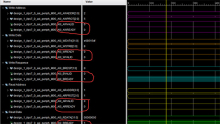
看完了AXI4-Full总线的仿真波形,我们再看下上面具体解析代码(可以理解为底层驱动)的仿真波形。按如下方法添加:

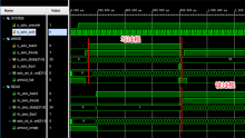
将信号按通道或用途做好分类,写事务的仿真结果如下:

读事务的仿真结果如下:

写入的数据与读出的数据一致。
可以看到其实AXI4-Full总线的使用还是相对比较简单的,只要设计好各个通道的握手时序,以及读写的时序关系就好了。下一篇文章我们再继续分析AXI4-Full总线的Master接口的代码。